Manufacturing
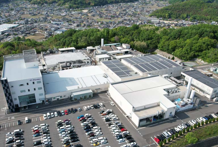
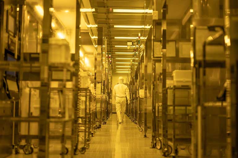
Phenitec provides foundry services in Japan using 5-inch and 6-inch lines for integrated manufacturing from epitaxial growth to wafer process, wafer inspection and testing.
We provide services and products that contribute to the further development of our customers with the technological capability and adaptability that we have cultivated since the founding of the company.
We provide services and products that contribute to the further development of our customers with the technological capability and adaptability that we have cultivated since the founding of the company.
Manufacturing capacity
Okayama Fab 1

Wafer manufacturing capacity
5 inch, 29,000 pcs/month (diodes, transistors, etc.)
6 inch, 27,000 pcs/month (MOSFETs, transistors, etc.)
6 inch, 27,000 pcs/month (MOSFETs, transistors, etc.)
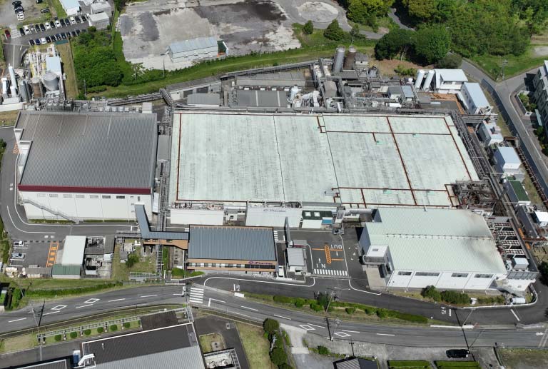
Kagoshima Fab

Wafer manufacturing capacity
6 inch, 19,000 pcs/month (CMOS ICs, MOSFETs, etc.)
Custom products
IC
- CMOS
- Bipolar
- Mixed-signal
- Sensor
- Trimming
- Up to medium voltage
Power MOSFETs
- Planar
- Trench
- SJ
- Up to 1200V
IGBT
- Planar
- Trench
- PT
- NPT
- FS
- Up to 3000V
Transistors
- Small-signal
- Fast-switching
- Up to 500 V
- JFET
Diodes
- PN
- SB
- Photo
- Fast-switching
- Up to 1600V
TVS
- Planar
- Trench
- Ultralow capacitance
Compounds
- SiC
- GaN
- GaAs
- Ga2O3
MEMS
Partial process
Custom processes
Deposition
Epitaxy
- Single-wafer
- Batch
- Boron
- Phosphorus
- Up to 50um
Oxidation
- Dry
- Wet
- Pyrogenic
SOG
- Non-dope
- Boron
- Antimony
CVD
- SiO
- SiN
- TEOS
- SiON
- PSG
- BPSG
- PolySi
- W
- Doped-PolySi
Sputtering/Evaporation/Plating
- Al
- AlSi
- AlCu
- AlSiCu
- Ti
- TiN
- WSi
- Mo
- Ni
- Au
- Ag
- Pt
- Si
Photo
- i-line
- g-line
- MPA
- Positive resist
- Polyimide
- Negative resist
Diffusion
Annealing
- Furnace
- Lamp
- Heavy-metal diffusion
- Phosphorus deposition
Etching
- Dry
- Wet
- Deep-trench
CMP
- SiO
- W
- Si
Ion implantation
- High energy
- Medium current
- High current
- B+
- P+
- As+
- Sb+
- BF2+
Wafer Test
- Logic
- Analog
- Up to 2000V
- Laser trimming
Backside processing
Dicing
Process technology
Process
- 0.35um and up
Planarization
- CMP
- SOG
Metal wiring
- Structure up to 4 metals
- W-plug
- Lift-off
Backside processing
- 70um and up
- Grind
- Si etching
- Ion implantation
- Laser annealing
- TAIKO
CMOS shuttling

Phenitec offers a CMOS shuttle service that can be used jointly by multiple customers or for the development of multiple chips.
Prototyping is available at a reasonable range by having multiple customers in the same reticle.
Overview
- Double-well 1P3M CMOS process
- Power supply voltage of 5 V
- Smallest gate length of 0.6um
Environments
Platforms

Chip size: 3.6 x 3.6 (mm)
LQFP 80-pin model
80PAD (fixed coordinates)

Chip size: 1.8 x 1.8 (mm)
LQFP 80-pin model
80PAD (fixed coordinates)
Design environments
- Design rule tables
- Spice parameter files
- User manuals
- Cadence technology files
- Jedat SX-Meister® initialization and verification rule files
- Siemens Calibre® verification rule files
- Sample layout [PAD cells (including ESD protection devices), resistors, capacitance, diodes]
- Logic synthesis and auto placement/wiring tools supported (GDS/, DB/LEF/.LIB)

CONTACT
Contact us for any questions about our products, services, recruitment, or anything else!